

基材
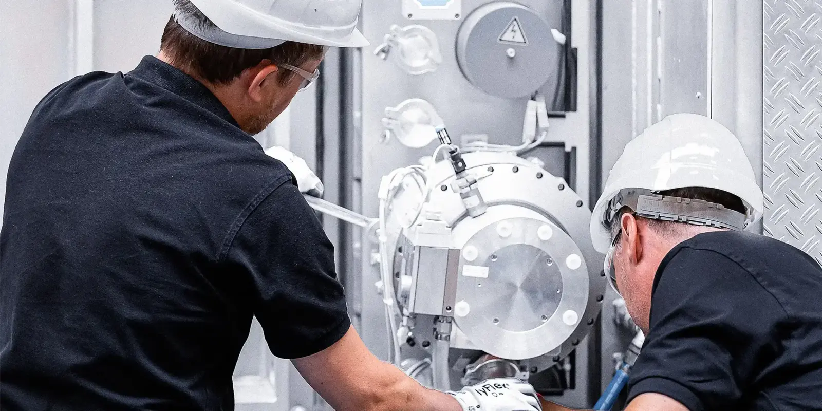
高精度涂层是精密光学的前提条件。它们利用干涉特性并提供所需的性能。基于我们的经验,VON ARDENNE 理解光学元件真空涂层所必需的物理过程。我们还具备将这些过程应用于各种不同基底形状和尺寸的专业知识。
基于我们的经验,VON ARDENNE 理解光学元件真空涂层所必需的物理过程。我们拥有将这些过程应用于各种不同基底形状和尺寸的专业知识。

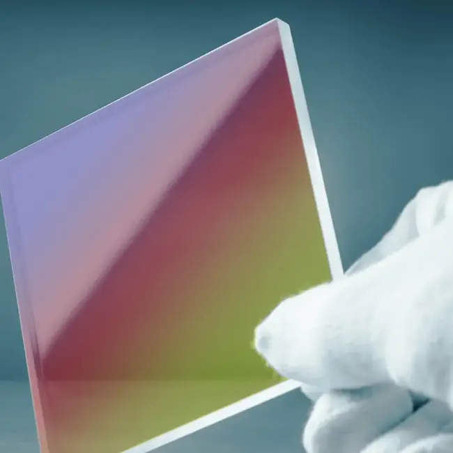
超薄玻璃
0.1 ~ 0.3 mm 厚度
Ø 200 mm

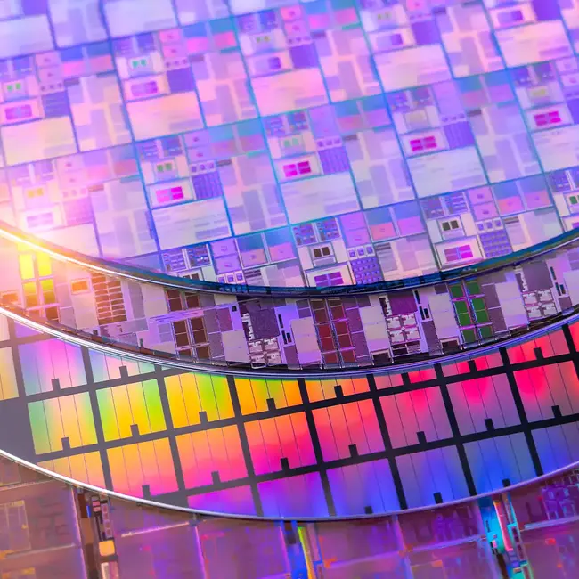
晶片级光学器件
3D传感器
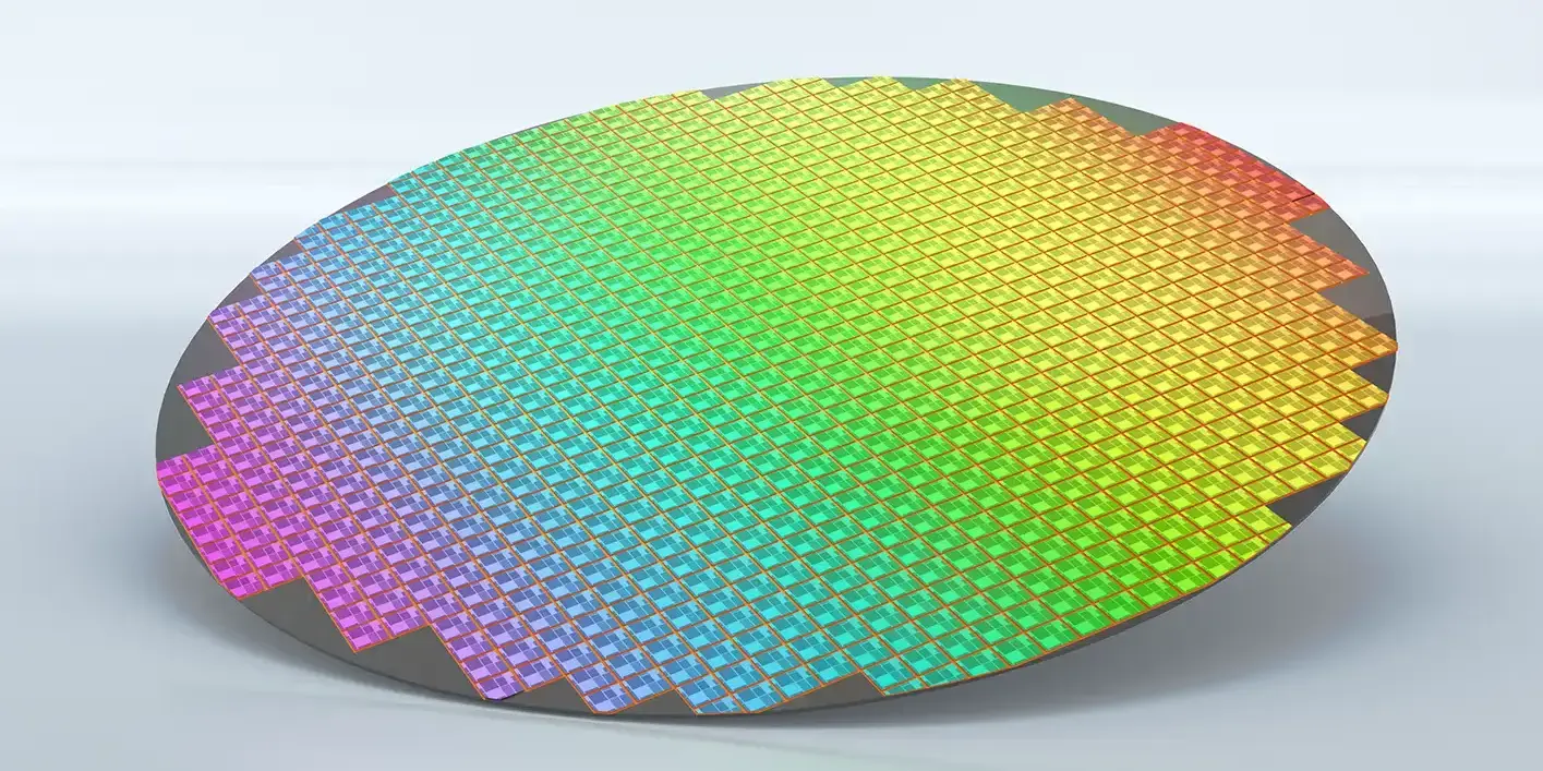
晶片 (Si, InP, GaAs)
0.7 mm厚度
Ø 4″, 6″, 200/300 mm
晶片级光学器件
激光二极管
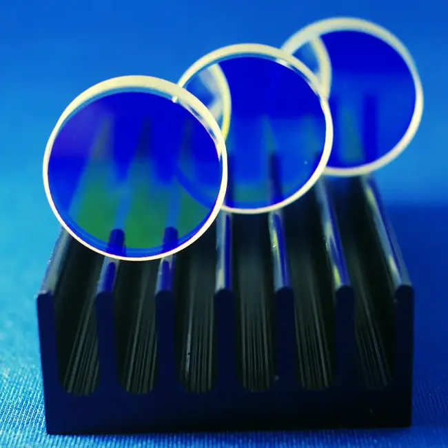
标准
1.0~6.5 mm厚度
Ø1″, 2″, 25/50 mm
□ 50x50/100x100 mm²
Catalog optics
激光光学

WEDGED-SHAPE
Like standards but with
nonparallel surfaces
(Δ << 1°)
Catalog optics
Laser optics
LARGE AREA
2~50 mm thick
Ø up to 200 mm
□ up to 300x400 mm²
AV/VR/XR
Automotive, HUD
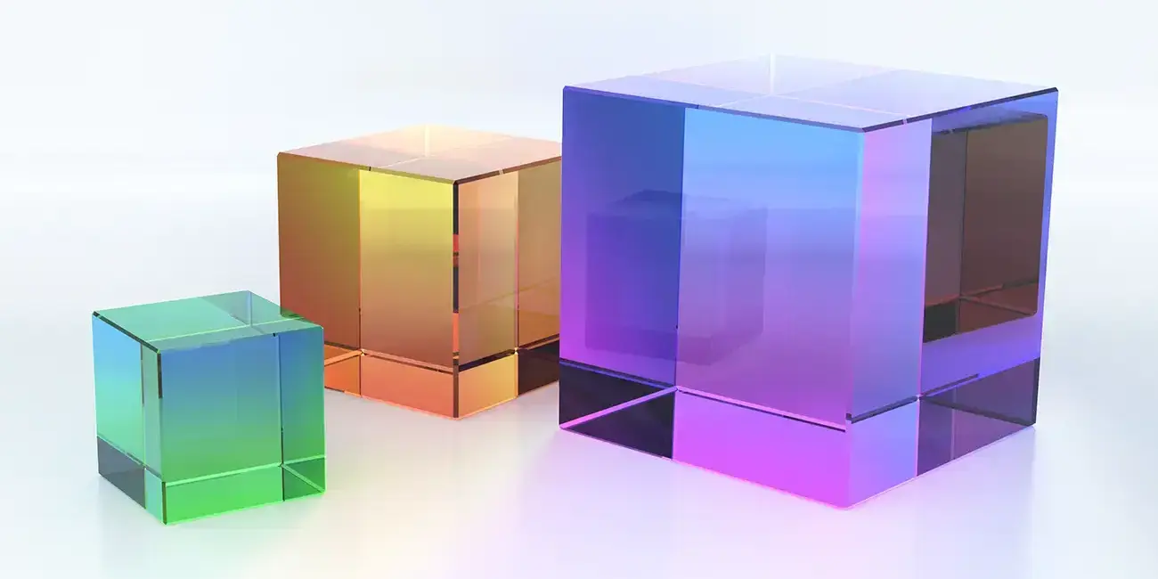
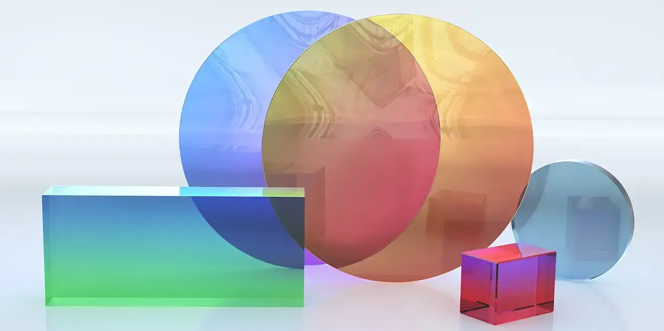
CUBICAL
5x5x5 mm³ up to
70x70x70 mm³
Telecom optics
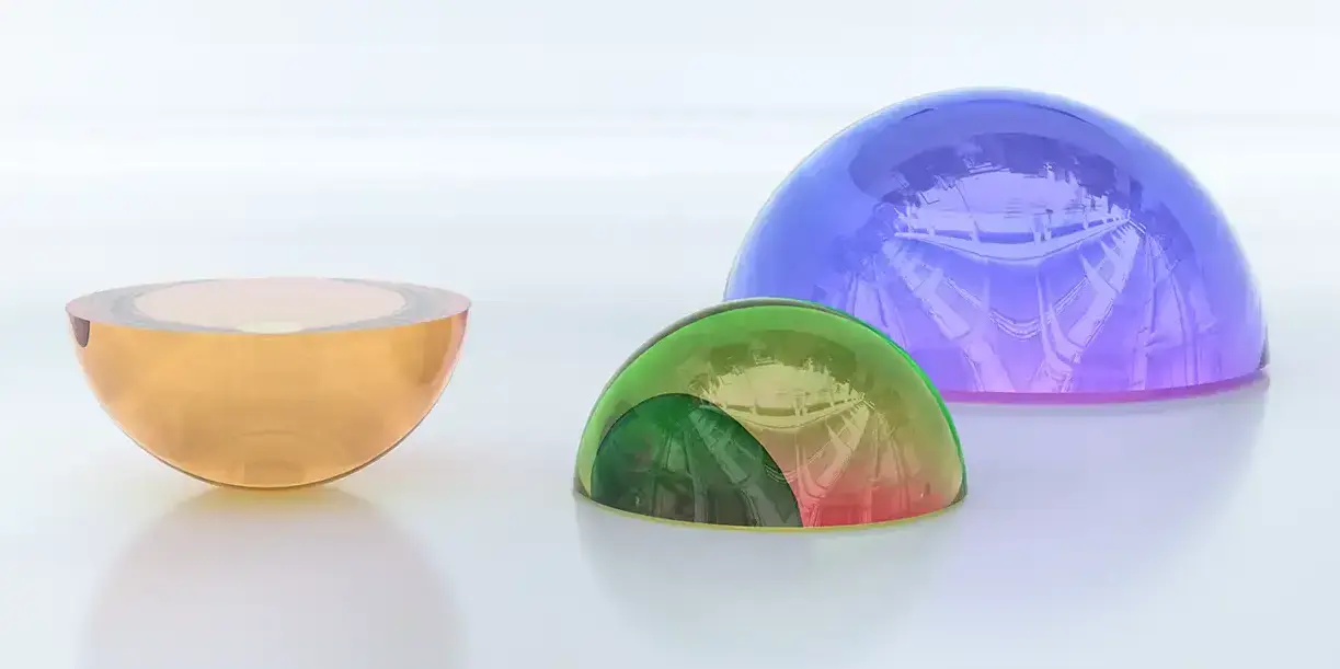
SPHERICAL
5-70 mm thick
Ø up to 200 mm
Laser optics
X-ray/EUV optics
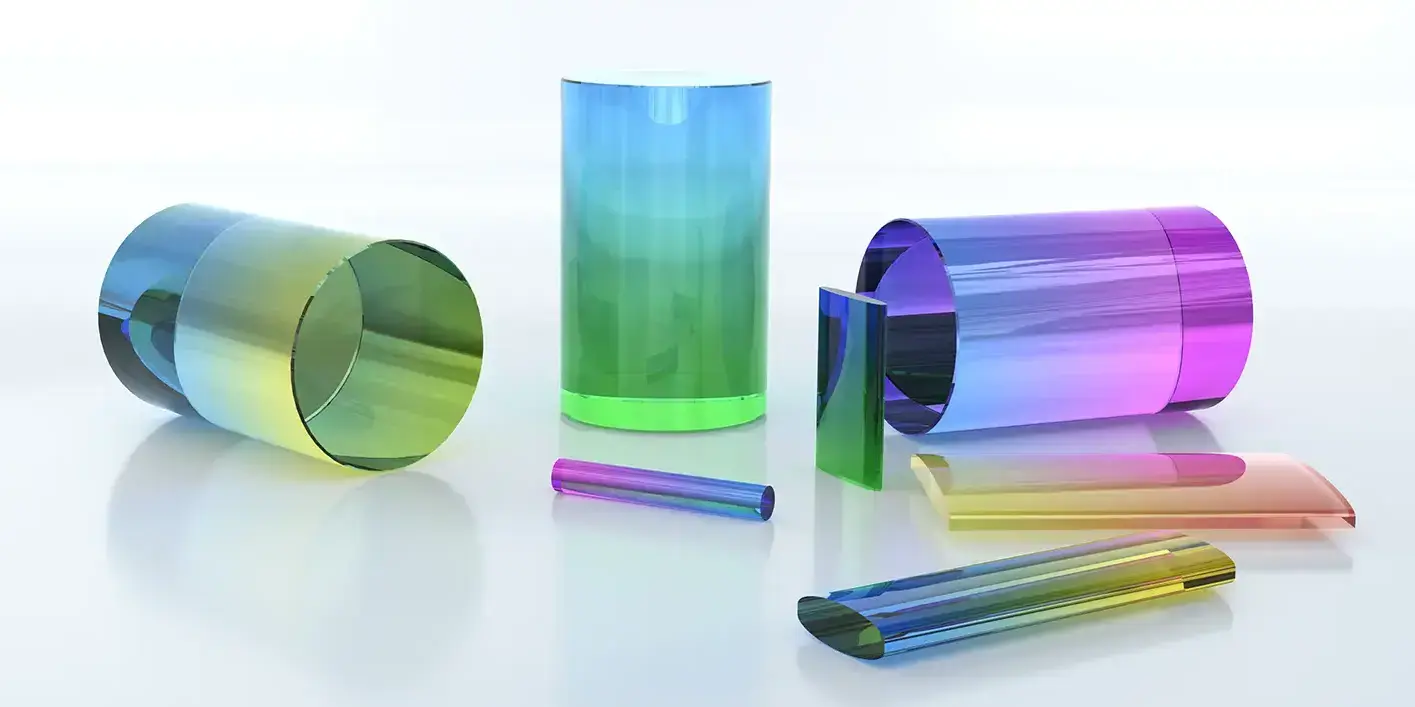
CYLINDRICAL
up to 70 mm thick
up to 200 mm wide
Laser optics
X-ray/EUV optics
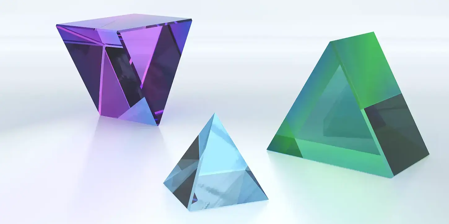
PRISM
Up to 70 mm
edge length
Catalog optics
Periscope optics
for precision optics, photonics & semiconductor applications
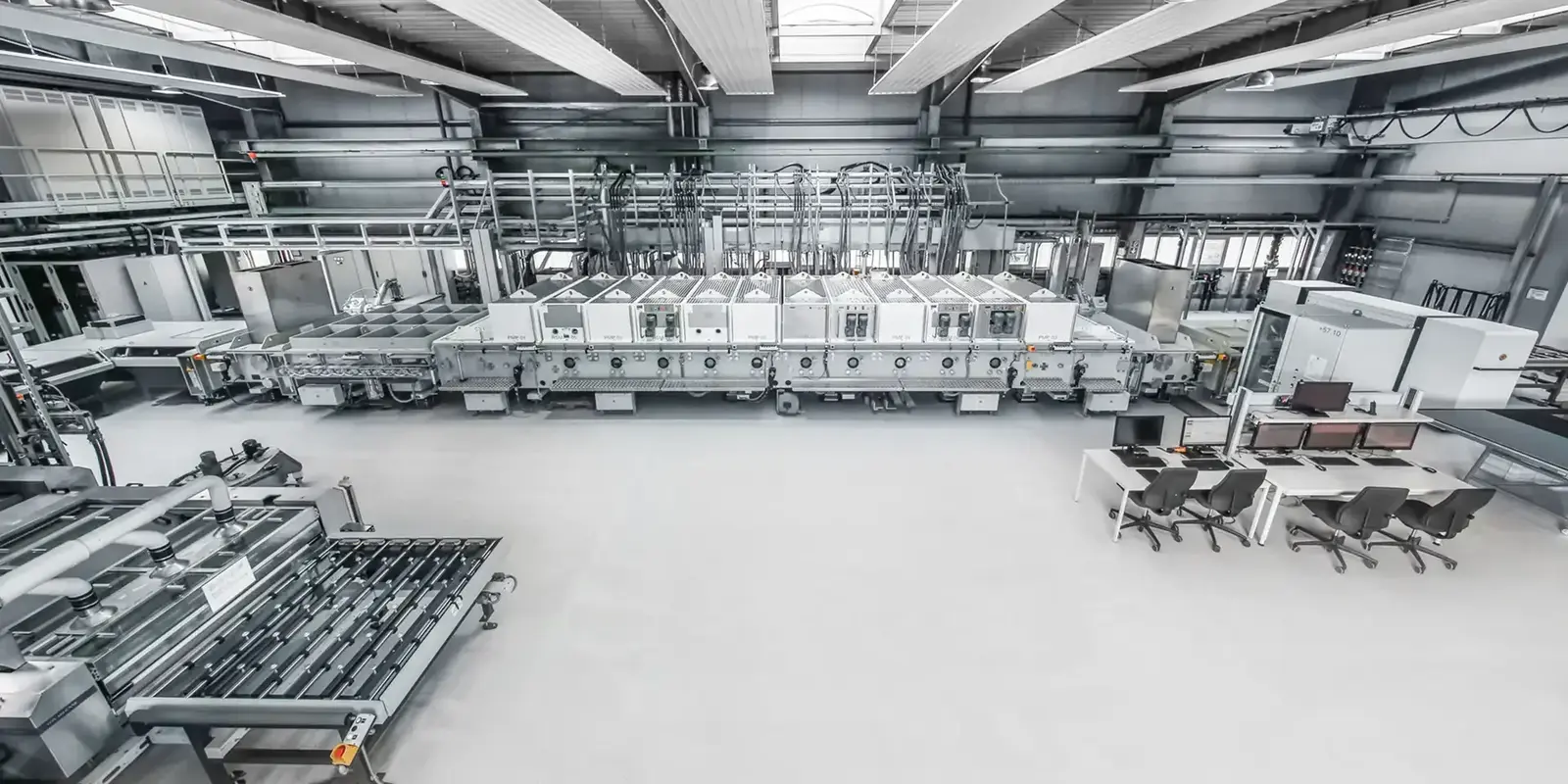
- Manufacturing of vacuum coating systems
- Sampling & pilot deposition services
- 600 m² semiconductor cleanroom including AMC capability
Dresden, Germany
International Congress Center
Booth F3
Dubai, United Arab Emirates
Dubai International Convention & Exhibition Centre
German Pavillon
Deputy Head of SalesVON ARDENNE Vacuum Equipment (Shanghai) Co., Ltd.